QCX assembly Rev 1.08. 113. Some excellent background reading are two papers by Paul Harden NA5N: aoc.nrao/~pharden/hobby/_ClassDEF1.pdf and.
138 pages
357 KB – 138 Pages
PAGE – 1 ============
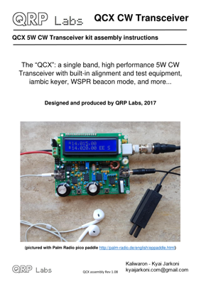
QCX assembly Rev 1.0 8 1 QCX CW Transceiver QCX 5W CW Transceiver kit assembly instructions ingle band, high performance 5W CW Transceiver with built – in alignment and test equipment, iambic keyer, WSPR beacon mode, and more Designed and produced by QRP Lab s, 2017 (pictured with Palm Radio pico paddle http://palm – radio.de/english/eppaddle.html )
PAGE – 2 ============
QCX assembly Rev 1.0 8 2 Contents 1. Introduction .. .. .. .. 5 2. Parts list .. .. .. .. .. .. 6 3. Assembly .. .. .. .. .. 7 3.1 Inventory parts .. .. .. .. . 13 3.2 Install IC2 socket .. .. .. .. . 14 3.3 Install DIP integrated circuits IC3, IC5 – 10 .. .. .. .. 14 3.4 Install all 100 nF (0.1uF) capacitors .. .. .. .. 15 3.5 Install all 470nF capacitors .. .. .. 16 3.6 Install all 1nF capacitors .. .. .. .. .. 17 3.7 Install all 10nF capacitors .. .. .. .. 17 3.8 Install 47nF capacitors .. .. .. .. . 18 3.9 Install 39nF capacitor .. .. .. .. 18 3.10 Install 2.2nF capacitors .. .. .. .. 19 3.11 Install 33nF and 3.3nF capacitors .. .. .. .. 19 3.12 Install capacitors C25 and C26 from the Low Pass Filter kit .. .. .. 20 3.13 Install capacitors C27 and C28 from the Low Pass Filter kit .. .. .. 21 3.14 Install capacitor C30 .. .. .. .. .. 22 3.15 Install capacitors C5 and C8 .. .. .. . 23 3.16 Install 1uF capacitor .. .. .. .. .. 24 3.17 Install 1N4148 diodes .. .. .. .. 24 3.18 Install 1N5819 diode .. .. .. .. . 25 3.19 Install 20MHz crystal XTAL1 .. .. .. . 26 3.20 Install 27MHz crystal XTAL2 .. .. .. . 27 3.21 Install all 10K resistors .. .. .. .. . 27 3.22 Install all 1K resistors .. .. .. .. 28 3.23 Install all 3.3K resistors .. .. .. .. 29 3.24 Install all 100 – ohm resistors .. .. .. . 29 3.25 Install 120K resistors .. .. .. .. . 30 3.26 Install 33K resistors .. .. .. .. 30 3.27 Install 47K resisto rs .. .. .. .. 31 3.28 Install 36K resistors .. .. .. .. 31 3.29 Install 270 – ohm resistor R48 .. .. .. 32 3.30 Install 470 – ohm resistor R41 .. .. .. 32 3.31 Install 3.9K resistor R61 .. .. .. .. 33 3.32 Install 4.3K resistor R18 .. .. .. .. 33 3.33 Install 5.1K resistor R11 .. .. .. .. 34 3.34 Install 7.5K resistor R21 .. .. .. .. 34 3.35 Install 750K resistor R35 .. .. .. .. .. 35 3.36 Install 100K trimmer potentiometer R47 .. .. .. .. 35 3.37 Install 500 – ohm multi – turn trimmer potentiometer .. .. .. 36 3.38 Install 50K multi – turn trimmer potentiomers .. .. .. . 36 3.39 Install two 100uH inductors .. .. .. . 37 3.40 Install 10uF capacitors .. .. .. .. . 38 3.41 Install 220uF capacitor C47 (may be supplied as 470uF) .. .. . 39 3.42 Install 30pF trimme r capacitor C1 .. .. .. . 40 3.43 Install MPS2907 transistor Q6 .. .. .. Error! Bookmark not defined. 3.44 Install all BS170 transistors .. .. .. .. 41 3.45 Install 2×3 – pin in – circuit programming header .. .. . 41
PAGE – 3 ============
QCX assembly Rev 1.0 8 3 3.46 Install 4 – pin GPS header .. .. .. .. .. 42 3.47 Install 3 – pin DVM/RF detector header .. .. .. 42 3.48 Install 1 – pin test points .. .. .. .. 43 3.49 Install power connector .. .. .. .. .. 43 3.50 Install 7805 voltage regulator IC11 .. .. .. .. 44 3.51 Install pin headers for the LCD module .. .. .. .. 44 3.52 Wind and install toroid L4 .. .. .. . 45 3.53 Wind and install toroid L2 .. .. .. . 47 3.54 Wind and install toroids L1 and L3 .. .. .. 48 3.55 Wind and install transformer T1 .. .. .. 49 3.56 Install RF output BNC connector .. .. .. 55 3.57 Install 3.5mm stereo connectors .. .. .. .. 56 3.58 Install buttons S2 and S3 (left and right buttons) .. .. 56 3.59 Install rotary encoder .. .. .. .. 57 3.60 Install microswitch .. .. .. .. . 57 3.61 Install gain control potentiometer R36 .. .. .. .. 58 3.62 Install four 12mm hex spacers at the LCD corners .. .. . 59 3.63 Install four 12mm hex spacers at the PCB corners .. .. . 59 3.64 Install knobs .. .. .. .. .. 60 3.65 Install 16 – pin female connector on LCD module .. .. .. 60 3.66 Install microcontroller .. .. .. .. .. 60 3.67 Install LCD and the remaining 4 screws to bolt LCD module .. .. . 60 3.68 Connections for off – board mounting of controls .. .. . 61 3.69 Connections for basic operation .. .. .. 62 3.70 Adjustment and alignment .. .. .. .. 63 4. Operating instructi ons .. .. .. .. 67 4.1 Overview of features .. .. .. .. . 67 4.2 Display elements .. .. .. .. . 69 4.3 Oper ator controls .. .. .. .. 70 4.4 Tune rate .. .. .. .. . 70 4.5 Keyer speed .. .. .. .. 71 4.6 RIT .. .. .. .. .. 71 4.7 VFO mode .. .. .. .. 72 4.8 VFO A/B frequency swap .. .. .. .. 72 4.9 Frequency Presets .. .. .. .. .. 72 4.10 Automated message transmission mode .. .. .. . 73 4.11 Menu System .. .. .. .. 73 4. 12 Saving current operating parameters (VFO frequency etc) .. .. 74 4.13 Types of configuration menu item .. .. .. 75 4.14 Editing a configuratio n menu parameter .. .. .. .. 75 4.15 Editing a LIST parameter .. .. .. .. . 75 4.16 Editing a BOOLEAN parameter .. .. .. 75 4.17 Editing a NUMBER parameter .. .. .. . 76 4.18 Editing a TEXT parameter .. .. .. .. 76 4.19 Frequency presets menu .. .. .. .. . 78 4.20 Messages menu .. .. .. .. .. 78 4.21 VFO menu .. .. .. .. 79 4.22 Keyer menu .. .. .. .. 81 4.23 Decoder menu .. .. .. .. .. 85 4.24 Beacon menu .. .. .. .. 87 4.25 Other menu .. .. .. .. 94
PAGE – 4 ============
QCX assembly Rev 1.0 8 4 4.26 Alignment menu .. .. .. .. .. 96 4.27 Test equipment .. .. .. .. . 10 0 5. Circuit design .. .. .. .. . 104 5.1 Block diagram and summary .. .. .. . 104 5.2 Circuit diagram .. .. .. .. .. 106 5.3 Synthesised oscillator .. .. .. .. . 106 5.4 Transmit/Receive switch .. .. .. . 107 5.5 Band Pass, Phase Splitter, QSD and pre – amps .. .. 108 5.6 90 – degree audio phase shift .. .. .. . 109 5.7 CW filter .. .. .. .. 110 5.8 Audio amplifier .. .. .. .. .. 110 5.9 Transmit signal routing and PA driver .. .. .. .. 112 5.10 Class – E Power Amplifier .. .. .. .. 112 5.11 Low Pass Filter .. .. .. .. 114 5.12 Key – shaping circuit .. .. .. .. .. 114 5.13 Microcontroller .. .. .. .. . 116 5.14 Optiona l GPS interface .. .. .. .. .. 119 5.15 In Circuit Programming (ISP) interface .. .. .. . 120 5.16 Test Equipment .. .. .. .. . 120 5.17 5V voltage regulator .. .. .. .. 123 6. Fault – finding .. .. .. .. .. 123 6.1 Blank LCD or blocked LCD .. .. .. .. 123 6.2 No backlight at all .. .. .. .. . 123 6.3 A row of blocks appears on the top row .. .. .. . 124 6.4 DC voltag e readings .. .. .. .. 124 6.5 RF Power output check .. .. .. .. . 126 6.6 Audible continuous clicking noise during receive .. .. . 127 7. Measurements .. .. .. .. . 127 7.1 Equipment .. .. .. .. 128 7.2 Transceiver current consumption .. .. .. .. 128 7.3 Transmitter power output .. .. .. . 129 7.4 Class – E Power Amplifier drain waveform .. .. .. 130 7.5 RF envelope key – shaping .. .. .. 130 7.6 Low Pass transmitter harmonic output filter characteristics .. .. . 131 7.7 Band Pass receiver input filte r characteristics .. .. 131 7.8 Quadrature Sampling Detector bandwidth .. .. .. .. 134 7.9 CW Filter response .. .. .. .. .. 135 7.10 Unwanted sideband rejection .. .. .. .. 136 8. .. .. .. 137 9. Resources .. .. .. .. 138 10. Document Revision History .. .. .. . 138
PAGE – 5 ============
QCX assembly Rev 1.0 8 5 1. Introduction Thank you for purchasing this high performance single – band 5W CW transceiver kit , the QCX (for Q RP Labs C W X cvr) . T his kit has a long list of features! Easy to build, single – board design, 10 x 8cm, all controls are board – mounted Professional quality double – sided, through – hole plated, silk – screen printed PCB Choice of single band, 80, 60, 40, 30, 20 or 17 m Approximatel y 3 – 5 W CW output (depending on supply voltage) 7 – 16 V recommended supply voltage 7 – element Low Pass Filter ensure s regulatory compliance CW envelope shaping remove s key clicks High perfor mance receiver with at least 50 dB of unwanted sideband cancellation 200Hz CW filter with no ringing Si5351A Synthesized VFO with rotary encoder tuning 16 x 2 blue backlight LCD screen Iambic keyer or straight key option included in the firmware Simple Digi tal Signal Processing assisted CW decoder, displayed real – time on – screen On – screen S – meter Full or semi QSK operation using fast solid – state transmit/receive switching Frequency presets, VFO A/B Split operation, RIT, configurable CW Offset Configurable sid etone frequency and volume Connectors: Power, 3.5mm keyer jack, 3.5mm stereo earphone jack, BNC RF output Onboard microswitch can be used as a simple straight Morse key Built – in test signal generator and alignment tools to complete simple set – up adjustme nts Built – in test equipment: voltmeter, RF power meter, frequency counter, signal generator Beacon mode, supporting automatic CW or WSPR operation GPS interface for reference frequency calibration and time – keeping (for WSPR beacon) No test equipment is req uired to build, align and operate this CW transceiver. Its innovative self – alignment and self – test features will help and guide you in setting up the transceiver in a few easy steps. The kit also includes a voltmeter, RF power meter, frequency counter and signal generator which can aid in debugging and fault – finding. We hope you enjoy building and operating this kit! Please read this assembly manual carefully, and follow the instructions step by step in the recommended order. Later in the manual the circuit design is described in detail and we recommend reading and understanding this section too, to get the maximum enjoyment and education from your new radio. Typical performance measurements are shown in the measurements section. The operation section of th e manual describes transceiver, alignment and test equipment operation in detail.
PAGE – 6 ============
QCX assembly Rev 1.0 8 6 2. Parts list Resistors (all fixed resistors are ¼ – Watt, 1% tolerance) R5 , R6, R8, R9 100 – ohm (4 pcs) , brown – black – black – black – brown R48 270 – ohm , red – purple – black – black – brown R41 470 – ohm , yellow – purple – black – black – brown R3, 4, 19 , 26, 37, 42 , 45, 53 – 55 , 62, 63 1K (12 pcs) , brown – black – black – brown – brown R12, 13, 15, 16, 20, 22, 23 , 25, 4 4, 56, 59 3.3K (11 pcs) , orange – orange – black – brown – brown R61 3.9K , orange – white – black – brown – brown R18 4.3K , yellow – orange – black – brown – brown R11 5.1K , green – brown – black – brown – brown R21 7. 5 K , purple – green – black – brown – brown R1 , 2, 7, 10, 14, 34, 39, 40 , 46, 49 – 52, 57, 58 10K (15 pcs) , brown – black – black – red – brown R28 , 29 33K (2 pcs) , orange – orange – black – red – brown R30 , 31 47K (2 pcs) , yellow – purple – black – red – brown R32 , 33 36K (2 pcs) , orange – blue – black – red – brown R38, 43, 6 0 120K (3 pcs) , brown – red – black – orange – brown R35 750K , purple – green – black – orange – brown R27 500 – ohm multi – turn trimmer potentiometer R17, 24 50K multi – turn trimmer potentiometer (2 pcs) R36 5K Log arithmic potentiomete r R47 100K trimmer potentiometer Capacitors C5 22pF (not used on every band version) C30 30pF (not used on every band version) C8 39pF (not used on every band version) C14 , 16, 18 , 23, 33 1nF (5 pcs) C19 , 20 2.2nF (2 pcs) C53 3.3nF C4 , 7, 10 , 42 10nF (4 pcs) C15 33nF C17 39nF C9 , 13 47nF (2 pcs) C2 , 3, 6, 12 , 29, 32 , 34 – 36, 39 – 41, 48 – 50, 52 0.1uF (16 pcs) C11 , 43 – 46 470nF (5 pcs) C31 1uF C21 , 2 2 , 24 , 37, 38, 51 10uF electrolytic (6 pcs) C47 470uF electrolytic C25 , C26 Value depends on band , in LPF kit bag (2 pcs) C27, C28 Value depends on band, in LPF kit bag (2 pcs) C1 30pF trimmer Semiconductors D1 , 2, 4, 5 1N4148 (4 pcs) D3 1N5819
PAGE – 8 ============
QCX assembly Rev 1.0 8 8 nts and soldered joints a fine – tipped soldering iron too. It is good to get into the habit of inspecting every joint with the (like this one I use) , right after soldering. This way you can easily identify any dry joints or solder bridges, before they become a problem later on when you are trying to test the project. Triple check every component value and location BEFORE soldering the component! It is easy to put component leads into the wrong holes, so check, check and check again! It is difficult to de – solder and replace comp onents, so it is much better to get them correctly installed the first time. In the event of a mistake, i t is always best to detect and correct any errors as early as possible (immediately after soldering the incorrect component). Again , a reminder: r emovi ng a component and re – installing it later is often very difficult! All of the resistors in the kit are installed vertically, because PCB space is limited. You will need to bend the resistor wires as shown in the picture below. On the parts layout diagram , there is a small circle around the hole where the body end of the resistor should be installed. This is not that the folded over wire – end of the resist wire or metal part. Please refer to the layout diagram and PCB tracks diagrams below, and follow the steps carefully. Assembly steps will be in the order of smallest to largest components. I follow the order semiconductors, capa citors, resistors and finally all other (generally larger) components. It is probably unnecessarily thorough and complex to build the radio one stage at a time and test each As per stand ard QRP Labs practice, the ATmega328P microcontroller has a 28 – pin DIP socket in case you may wish to subsequently replace it for firmware upgrades etc. The Si5351A and FST3253 ICs are only available in surface mount packages so these are already soldered to the PCB for you, at the factory. All other components used are al l leaded through – hole packages, and all are installed on the top side of the PCB. Personally , I believe that on average, the use of IC sockets causes more problems than it solves. socket, issues with increased lead length, etc. Accordingly, the remaini ng ICs are soldered directly into the PCB without IC sockets. Please forgive me if you disagree. You may find it convenient to inventory the resistors and capacitors and sort them by value, so that you can easily find the correct ones as you work through the assembly steps.
PAGE – 11 ============
QCX assembly Rev 1.0 8 11 The PCB track and circuit (schematic) diagram s are shown on the previous page s . Tracks shown in BLUE are on the bottom layer. Tracks shown in RED are on the top layer. There are only two layers (nothing is hidden in the middle). Not shown in this diagram are the extensive ground – planes , on both sides of the board . Practically e verything on both layer s or BLUE track, is ground – plane! The two ground – planes are connected at frequent intervals (not more than 0.1 – inches) by vias. This is the kind of layout I have done previously for a quad – band GSM device I used to say often that you can never have too much supply line filter ing and decoupling, and do to homebrew projects. In a kit every decoupling capacitor has a cost in both money and PCB area (which also means more money). Shiel ding is even more difficult and expensive. So shielding and decoupling should be applied where needed only! But ground – plane so put it everywhere. The PCB silkscreen compo nent numbers are necessarily quite small and may be overlapping pads or vias, or near to other components. It may be nice to have doubled the size of the PCB and have more space to print nice silkscreen labels of the component numbers. But the result would So check carefully, before soldering each component! Check the location and check again with reference to the diagrams in each step. All components are installed on t he top (component side) of the PCB and soldered on the bottom (solder side) of the PCB. Take care when installing integrated circuits. All through – hole integrated circuits are supplied by the manufacturers with their pins bent a little wide. You need to c arefully bend the rows of pins together a little, in order to fit them in the PCB holes, or in the 28 – pin IC socket in the case of the ATmega328P microcontroller. The band – specific Low Pass Filter (LPF) parts are supplied in a separate LPF kit bag. In the construction for some bands, not all of the capacitors supplied in the kit are used. D o not be alarmed if you have a few components left over at the end ! Wind the L1 – 3 inductors with the enamelled copper wire supplied in the LPF kit bag. Wind the other in ductors (L4 and transformer T1) using the wire supplied in the main kit bag. The component colour coding of the layout diagram at every step of the assembly instructions is as follows ( kind of: components past, present and future): Components shaded grey have already been installed Components shaded red are the ones being installed in the current assembly step Components shaded white are the ones which have not yet been installed The following photographs show the final assembly, with and without the LCD module plugged in. You can keep these photographs in mind when assembling the kit, they will give you some idea of how the kit fits together and help avoid assembly errors.
357 KB – 138 Pages