The transient detection function can be routed to either interrupt pin through bit 5 in CTRL_REG5 register (0x2E). registers 0x1D to 0x20 are the dedicated
130 KB – 54 Pages
PAGE – 1 ============
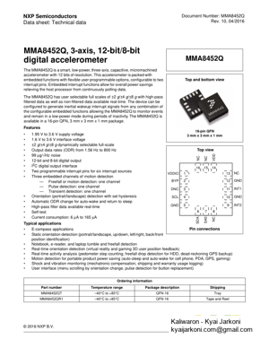
Document Number: MMA8452Q Rev. 10, 04/2016 NXP SemiconductorsData sheet: Technical data © 2016 NXP B.V. MMA8452Q, 3-axis, 12-bit/8-bit digital accelerometerThe MMA8452Q is a smart, low-power, three-axis, capacitive, micromachined accelerometer with 12 bits of resolution. This accelerometer is packed with embedded functions with flexible user programmable options, configurable to two interrupt pins. Embedded interrupt functions allow for overall power savings relieving the host processor from continuously polling data. The MMA8452Q has user select able full scales of ±2 g/±4 g/±8 g with high-pass filtered data as well as n on-filtered data available real-time. The device can be configured to generate inertial wakeup interrupt signals from any combination of the configurable embedded functions allowing the MMA8452Q to monitor events and remain in a low-power mode during periods of inactivity. The MMA8452Q is available in a 16-pin QFN, 3 mm x 3 mm x 1 mm package. Features Ł1.95 V to 3.6 V supply voltage Ł1.6 V to 3.6 V interface voltage Ł±2 g/±4 g/±8 g dynamically selectable full-scale ŁOutput data rates (ODR) from 1.56 Hz to 800 Hz Ł99 µg/Hz noise Ł12-bit and 8-bit digital output ŁI2C digital output interface ŁTwo programmable interrupt pins for six interrupt sources ŁThree embedded channels of motion detection Š Freefall or motion detection: one channel Š Pulse detection: one channel Š Transient detection: one channel ŁOrientation (portrait/landscape) detection with set hysteresis ŁAutomatic ODR change for auto-wake and return to sleep ŁHigh-pass filter data available real-time ŁSelf-test ŁCurrent consumption: 6 µA to 165 µATypical applications ŁE-compass applications ŁStatic orientation detection (portrait/la ndscape, up/down, left/right, back/front position identification) ŁNotebook, e-reader, and laptop tumble and freefall detection ŁReal-time orientation detection (virtual r eality and gaming 3D user position feedback) ŁReal-time activity analysis (pedomet er step counting, freefal l drop detection for HDD, dead-reckoning GPS backup) ŁMotion detection for portable product power saving (aut o-sleep and auto-wake for cell phone, PDA, GPS, gaming) ŁShock and vibration monitoring (mechatronic compensation, shipping and warranty usage logging) ŁUser interface (menu scrolling by orientation change, pulse detection for button replacement) Ordering information Part number Temperature range Package description ShippingMMA8452QTŒ40°C to +85°C QFN-16 Tray MMA8452QR1Œ40°C to +85°C QFN-16 Tape and Reel MMA8452Q16-pin QFN 3 mm x 3 mm x 1 mm Top and bottom view Top view Pin connections 12345910111213141516876 NCVDDNCVDDIOBYPDNC SCLGNDNCGNDINT1 GNDINT2 SA0NCSDA
PAGE – 2 ============
MMA8452Q Sensors2NXP Semiconductors Related documentation The MMA8452Q device features and operations are described in a variety of reference manuals, user guides, and application notes. To find the most-current versions of these documents: 1.Go to the NXP homepage at: http://www.nxp.com/ 2.In the ALL search box at the top of th e page, enter the devic e number MMA8452Q. 3.Click the Documents link. Contents 1Block Diagram and Pin Description . . . . . . . . . . . . . . . . . . . . . . . . . . . . . . . . . . . . . . . . . . . . . . . . . . . . . . . . . . . . . . . . . 3 2Mechanical and Electrical Specifications. . . . . . . . . . . . . . . . . . . . . . . . . . . . . . . . . . . . . . . . . . . . . . . . . . . . . . . . . . . . . 6 2.1Mechanical characteristics . . . . . . . . . . . . . . . . . . . . . . . . . . . . . . . . . . . . . . . . . . . . . . . . . . . . . . . . . . . . . . . . . . . . . 6 2.2Electrical characteristics. . . . . . . . . . . . . . . . . . . . . . . . . . . . . . . . . . . . . . . . . . . . . . . . . . . . . . . . . . . . . . . . . . . . . . . 7 2.3I 2C interface characteristics . . . . . . . . . . . . . . . . . . . . . . . . . . . . . . . . . . . . . . . . . . . . . . . . . . . . . . . . . . . . . . . . . . . . 8 2.4Absolute maximum ratings . . . . . . . . . . . . . . . . . . . . . . . . . . . . . . . . . . . . . . . . . . . . . . . . . . . . . . . . . . . . . . . . . . . . . 9 3Terminology . . . . . . . . . . . . . . . . . . . . . . . . . . . . . . . . . . . . . . . . . . . . . . . . . . . . . . . . . . . . . . . . . . . . . . . . . . . . . . . . . . . 10 3.1Sensitivity . . . . . . . . . . . . . . . . . . . . . . . . . . . . . . . . . . . . . . . . . . . . . . . . . . . . . . . . . . . . . . . . . . . . . . . . . . . . . . . . . 10 3.2Zero- g offset . . . . . . . . . . . . . . . . . . . . . . . . . . . . . . . . . . . . . . . . . . . . . . . . . . . . . . . . . . . . . . . . . . . . . . . . . . . . . . . 10 3.3Self-test. . . . . . . . . . . . . . . . . . . . . . . . . . . . . . . . . . . . . . . . . . . . . . . . . . . . . . . . . . . . . . . . . . . . . . . . . . . . . . . . . . . 10 4System Modes (SYSMOD) . . . . . . . . . . . . . . . . . . . . . . . . . . . . . . . . . . . . . . . . . . . . . . . . . . . . . . . . . . . . . . . . . . . . . . . . 11 5Functionality . . . . . . . . . . . . . . . . . . . . . . . . . . . . . . . . . . . . . . . . . . . . . . . . . . . . . . . . . . . . . . . . . . . . . . . . . . . . . . . . . . . 12 5.1Device calibration . . . . . . . . . . . . . . . . . . . . . . . . . . . . . . . . . . . . . . . . . . . . . . . . . . . . . . . . . . . . . . . . . . . . . . . . . . . 13 5.28-bit or 12-bit data. . . . . . . . . . . . . . . . . . . . . . . . . . . . . . . . . . . . . . . . . . . . . . . . . . . . . . . . . . . . . . . . . . . . . . . . . . . 13 5.3Low-power modes vs. high-resolution modes. . . . . . . . . . . . . . . . . . . . . . . . . . . . . . . . . . . . . . . . . . . . . . . . . . . . . . 13 5.4Auto-wake/sleep mode. . . . . . . . . . . . . . . . . . . . . . . . . . . . . . . . . . . . . . . . . . . . . . . . . . . . . . . . . . . . . . . . . . . . . . . 13 5.5Freefall and motion detectio n . . . . . . . . . . . . . . . . . . . . . . . . . . . . . . . . . . . . . . . . . . . . . . . . . . . . . . . . . . . . . . . . . . 13 5.6Transient detection. . . . . . . . . . . . . . . . . . . . . . . . . . . . . . . . . . . . . . . . . . . . . . . . . . . . . . . . . . . . . . . . . . . . . . . . . . 14 5.7Pulse detection. . . . . . . . . . . . . . . . . . . . . . . . . . . . . . . . . . . . . . . . . . . . . . . . . . . . . . . . . . . . . . . . . . . . . . . . . . . . . 14 5.8Orientation detection. . . . . . . . . . . . . . . . . . . . . . . . . . . . . . . . . . . . . . . . . . . . . . . . . . . . . . . . . . . . . . . . . . . . . . . . . 14 5.9Interrupt register configurations . . . . . . . . . . . . . . . . . . . . . . . . . . . . . . . . . . . . . . . . . . . . . . . . . . . . . . . . . . . . . . . . 16 5.10Serial I 2C interface . . . . . . . . . . . . . . . . . . . . . . . . . . . . . . . . . . . . . . . . . . . . . . . . . . . . . . . . . . . . . . . . . . . . . . . . . . 16 6Register Descriptions. . . . . . . . . . . . . . . . . . . . . . . . . . . . . . . . . . . . . . . . . . . . . . . . . . . . . . . . . . . . . . . . . . . . . . . . . . . . 19 6.1Data registers . . . . . . . . . . . . . . . . . . . . . . . . . . . . . . . . . . . . . . . . . . . . . . . . . . . . . . . . . . . . . . . . . . . . . . . . . . . . . . 20 6.2Portrait/landscape embedded function registers. . . . . . . . . . . . . . . . . . . . . . . . . . . . . . . . . . . . . . . . . . . . . . . . . . . . 25 6.3Motion and freefall embedded function registers . . . . . . . . . . . . . . . . . . . . . . . . . . . . . . . . . . . . . . . . . . . . . . . . . . . 27 6.4Transient (HPF) acceleration detection . . . . . . . . . . . . . . . . . . . . . . . . . . . . . . . . . . . . . . . . . . . . . . . . . . . . . . . . . . 32 6.5Single, double and directional pulse-detection registers. . . . . . . . . . . . . . . . . . . . . . . . . . . . . . . . . . . . . . . . . . . . . . 34 6.6Auto-wake/sleep detection . . . . . . . . . . . . . . . . . . . . . . . . . . . . . . . . . . . . . . . . . . . . . . . . . . . . . . . . . . . . . . . . . . . . 39 6.7Control registers . . . . . . . . . . . . . . . . . . . . . . . . . . . . . . . . . . . . . . . . . . . . . . . . . . . . . . . . . . . . . . . . . . . . . . . . . . . . 40 6.8User offset correction registers. . . . . . . . . . . . . . . . . . . . . . . . . . . . . . . . . . . . . . . . . . . . . . . . . . . . . . . . . . . . . . . . . 43 7Printed Circuit Board Layout and Device Mounting . . . . . . . . . . . . . . . . . . . . . . . . . . . . . . . . . . . . . . . . . . . . . . . . . . . 47 7.1Printed circuit board layout. . . . . . . . . . . . . . . . . . . . . . . . . . . . . . . . . . . . . . . . . . . . . . . . . . . . . . . . . . . . . . . . . . . . 47 7.2Overview of soldering considerations. . . . . . . . . . . . . . . . . . . . . . . . . . . . . . . . . . . . . . . . . . . . . . . . . . . . . . . . . . . . 48 7.3Halogen content . . . . . . . . . . . . . . . . . . . . . . . . . . . . . . . . . . . . . . . . . . . . . . . . . . . . . . . . . . . . . . . . . . . . . . . . . . . . 48 8Package Information. . . . . . . . . . . . . . . . . . . . . . . . . . . . . . . . . . . . . . . . . . . . . . . . . . . . . . . . . . . . . . . . . . . . . . . . . . . . . 49 8.1Tape and reel information. . . . . . . . . . . . . . . . . . . . . . . . . . . . . . . . . . . . . . . . . . . . . . . . . . . . . . . . . . . . . . . . . . . . . 49 8.2Package description . . . . . . . . . . . . . . . . . . . . . . . . . . . . . . . . . . . . . . . . . . . . . . . . . . . . . . . . . . . . . . . . . . . . . . . . . 50 9Revision History . . . . . . . . . . . . . . . . . . . . . . . . . . . . . . . . . . . . . . . . . . . . . . . . . . . . . . . . . . . . . . . . . . . . . . . . . . . . . . . . 53
PAGE – 3 ============
SensorsNXP Semiconductors3MMA8452Q 1Block Diagram and Pin Description Figure1. Block diagram Figure2. Direction of the detectable accelerations 12-bitSDASCL I2CEmbedded DSPFunctionsC to VInternalOSC Clock GEN ADCConverter VDDIO VSSX-axis Transducer Y-axis Transducer Z-axis Transducer Freefall and Motion DetectionTransient Detection(i.e., fast-motion, transient) Orientation with Set Hysteresis and Z-lockout Shake Detection through MotionThreshold Auto-wake/auto-sleep configurable with debounce count er and multiple motion interrupts for control Auto-wake/sleep Active mode sleepVDDINT1 INT2 Active modewakeSingle, Double and Directional Tap Detection MODE OptionsLow Power Low Noise + Low Power High Resolution Normal MODE Options Low Power Low Noise + Low Power High Resolution Normal 1DIRECTION OF THE DETECTABLE ACCELERATIONS (BOTTOM VIEW) 5913XYZ1(TOP VIEW)Earth Gravity
PAGE – 4 ============
Sensors4NXP Semiconductors MMA8452Q Figure 3 shows the device configuration in the si x different orientation modes. These ori entations are defined as the following: PU = portrait up, LR = landscape right, PD = portrait down, LL = landscape left, back and front side views. There are several registers to configure the orientati on detection and are described in deta il in the register setting section. Figure3. Landscape/portrait orientation Figure4. Application diagram Top View PUEarth Gravity Pin 1Xout @ 0 gYout @ Œ1 gZout @ 0 gXout @ 1 gYout @ 0 gZout @ 0 gXout @ 0 gYout @ 1 gZout @ 0 gXout @ Œ1 gYout @ 0 gZout @ 0 gLLPDLRSide ViewFRONT Xout @ 0 gYout @ 0 gZout @ 1 gBACKXout @ 0 gYout @ 0 gZout @ Œ1 g0.1µF1.6V-3.6V VDDIOVDDIOVDDIO4.7k4.7k1GNDVDDIOSCL NCINT2 INT1 GNDGNDSDA SA0 VDDNCNCNCBYPNCMMA8452Q 21612131415 111034567894.7µFINT1 INT2 SA00.1µF1.95V-3.6V VDDSCLSDADNC
PAGE – 5 ============
SensorsNXP Semiconductors5MMA8452Q The device power is supplied through VDD line. Power supply decoupling capacitors (100 nF ceramic plus 4.7 µF bulk, or a single 4.7 µF ceramic) should be placed as near as po ssible to the pins 1 and 14 of the device. The control signals SCL, SDA, and SA0 are not tolerant of voltages more than VDDIO + 0.3 V. If VDDIO is removed, the control signals SCL, SDA, and SA0 will clamp any logic si gnals with their internal ESD protection diodes. The functions, the threshold and the timing of the two interrupt pins (INT1 and INT2) are user programmable through the I 2C interface. The SDA and SCL I 2C connections are open drain and therefore require a pullup resistor as shown in the application diagram in Figure 4 .Table1. Pin descriptions Pin #Pin name Description 1VDDIOInternal power supply (1.62 V to 3.6 V) 2BYPBypass capacitor (0.1 µF)3DNCDo not connect to anything, leave pin isolated and floating.4SCLI2C serial clock, open drain 5GNDConnect to ground 6SDA I2C serial data 7SA0 I2C least significant bit of the device I 2C address, I 2C 7-bit address = 0x1C (SA0 = 0), 0x1D (SA0 = 1). 8NCInternally not connected 9INT2Inertial interrupt 2, output pin 10GNDConnect to ground 11INT1Inertial interrupt 1, output pin 12GNDConnect to ground 13NCInternally not connected 14VDDPower supply (1.95V to 3.6V) 15NCInternally not connected 16NCInternally not connected (can be GND or VDD)
PAGE – 6 ============
Sensors6NXP Semiconductors MMA8452Q 2Mechanical and Electr ical Specifications 2.1Mechanical characteristics Table2. Mechanical characteristics @ VDD = 2.5V , VDDIO = 1.8V, T = 25°C unless otherwise noted .Parameter Test conditionsSymbolMinTypMaxUnit Measurement range (1) 1.Dynamic range is limited to 4 g when the low-noise bit in register 0x2A, bit 2 is set. FS[1:0] set to 002 g mode FSŠ±2Š gFS[1:0] set to 014 g modeŠ±4Š FS[1:0] set to 108 g modeŠ±8Š Sensitivity FS[1:0] set to 002 g mode SoŠ1024Š counts/ gFS[1:0] set to 014 g modeŠ512Š FS[1:0] set to 108 g modeŠ256Š Sensitivity accuracy (2)2.Sensitivity remains in spec as stated, but changing oversampling mode to low power causes 3% sensitivity shift. This behavior is also seen when changing from 800 Hz to any other data rate in the normal, low noise + low power or high resolution mode. ŠSoaŠ±2.64Š% Sensitivity change vs. temperature FS[1:0] set to 002 g mode TCSoŠ±0.008Š%/°C FS[1:0] set to 014 g modeŠŠFS[1:0] set to 108 g modeŠŠZero- g level offset accuracy (3) 3.Before board mount. FS[1:0] 2 g, 4 g, 8 g TyOffŠ±17Š mg Zero- g level offset accuracy post-board mount (4) 4.Post-board mount offset specifications ar e based on an 8-layer PCB, relative to 25°C. FS[1:0] 2 g, 4 g, 8 gTyOffPBMŠ±20Š mg Zero- g level change vs. temperature Œ40 °C to 85 °C TCOffŠ±0.15Š mg/°C Self-test output change (5) XY Z5.Self-test is one direction only. FS[1:0] set to 0 4 g mode Vst Š Š Š+44 +61+392Š Š Š LSBODR accuracy 2-MHz clockŠŠŠ±2Š %Output data bandwidthŠBWODR/3ŠODR/2 Hz Output noise Normal mode ODR = 400 HzNoiseŠ126Š µg/ HzOutput noise low-noise mode (1) Normal mode ODR = 400 HzNoiseŠ99Š µg/ HzOperating temperature range ŠTopŒ40Š+85 °C
PAGE – 8 ============
Sensors8NXP Semiconductors MMA8452Q 2.3I 2C interface characteristicsTable4. I 2C slave timing values (1) 1.All values referred to V IH(min) (0.3 V DD) and V IL(max) (0.7 VDD) levels. Parameter Symbol I2C fast-mode UnitMinMax SCL clock frequencyf SCL0400kHz Bus-free time between stop and start condition tBUF1.3 Šµs(Repeated) start hold timet HD;STA0.6 ŠµsRepeated start setup timet SU;STA0.6 ŠµsStop condition setup timet SU;STO0.6 ŠµsSDA data hold timet HD;DAT0.05 0.9(2) 2.This device does not stretch the low period (t LOW) of the SCL signal. µsSDA setup timet SU;DAT100ŠnsSCL clock low timet LOW1.3 ŠµsSCL clock high timet HIGH0.6 ŠµsSDA and SCL rise timet r20 + 0.1 Cb(3) 3.Cb = total capacitance of one bus line in pF. 300ns SDA and SCL fall timet f20 + 0.1 Cb(3) 300nsSDA valid time (4) 4.tVD;DAT = time for data signal from SCL low to SDA output (high or low, depending on which one is worse). tVD;DATŠ0.9(2) µsSDA valid acknowledge time (5) 5.tVD;ACK = time for acknowledgement signal from SCL low to SD A output (high or low, depending on which one is worse). tVD;ACKŠ0.9(2) µsPulse width of spikes on SDA and SCL that must be suppressed by internal input filter tSP050n sCapacitive load for each bus line CbŠ400pF
PAGE – 9 ============
SensorsNXP Semiconductors9MMA8452Q Figure5. I 2C slave timing diagram 2.4Absolute maximum ratings Stresses above those listed as absolute maximum ratings may cause permanent damage to the device. Exposure to maximum rating conditions for extended periods may affect device reliability. Table5. Maximum ratings Rating Symbol Value Unit Maximum acceleration (all axes, 100 µs)gmax 5,000gSupply voltageVDDŒ0.3 to + 3.6V Input voltage on any control pin (SA0, SCL, SDA)VinŒ0.3 to VDDIO + 0.3V Drop test Ddrop 1.8mOperating temperature range TOPŒ40 to +85 °C Storage temperature range TSTGŒ40 to +125 °CTable6. ESD and latchup protection characteristics Rating SymbolValueUnitHuman body modelHBM±2000VMachine model MM±200VCharge device model CDM ±500VLatchup current at T = 85°C Š±100mAVIL = 0.3VDDVIH = 0.7V DDThis device is sensitive to mec hanical shock. Improper handling can c ause permanent damage of the part or cause the part to otherwise fail. This device is sensitive to ESD, improper handling can cause permanent damage to the part.
PAGE – 10 ============
Sensors10NXP Semiconductors MMA8452Q 3Terminology 3.1Sensitivity The sensitivity is represented in counts/ g. In 2 g mode the sensitivity is 1024 counts/ g. In 4 g mode the sensitivity is 512 counts/ g and in 8 g mode the sensitivit y is 256 counts/ g.3.2Zero- g offsetZero-g offset (TyOff) describes the deviation of an actual output signal from the ideal output signal if the sensor is stationa ry. A sensor stationary on a horizontal surface will measure 0 g in X-axis and 0 g in Y-axis whereas the Z-axis will measure 1 g. The output is ideally in the middle of the dynamic range of the sensor (content of OUT registers 0x00, data expressed as 2’s complement number). A deviation from ideal value in this case is called zero- g offset. Offset is to some extent a result of stress on the MEMS sensor and therefore the offset can slightly cha nge after mounting the sensor onto a printed circuit board or exposing it to extensive mechanical stress. 3.3Self-test Self-test checks the transducer functionality with out external mechanical st imulus. When self-test is activated, an electrostat ic actuation force is applied to the sensor, si mulating a small acceleration. In this case, the sensor outputs will exhibit a chan ge in their DC levels which are related to the selected full scale thr ough the device sensitivity. When self-test is activated, the d evice output level is given by the algebraic sum of the signals produced by the acceleration acting on the sensor and by the electros tatic test-force.
PAGE – 11 ============
SensorsNXP Semiconductors11MMA8452Q 4System Modes (SYSMOD) Figure6. MMA8452Q mode transition diagram All register contents are preserved when transitioning from acti ve to standby mode. Some registers are reset when transitioning from standby to active. These are all noted in the device memo ry map register table. The sleep and wake modes are active modes. For more information on how to use the sleep and wake modes and how to transition between these modes, please refer to the functionality section of this document. Table7. Mode of operation description ModeI2C bus state VDDFunction description OFF Powered down <1.8V VDDIO Can be > VDD ŁThe device is powered off. ŁAll analog and digital blocks are shutdown. ŁI2C bus inhibited.StandbyI2C communication is possible >1.8V ŁOnly digital blocks are enabled. analog subsystem is disabled. ŁInternal clocks disabled. ŁRegisters accessible for read/write. ŁDevice is configured in standby mode. Active (wake/sleep) I2C communication is possible >1.8V ŁAll blocks are enabled (digital, analog). OFFWakeStandby OFFActiveSYSMOD = 00 SYSMOD = 10 SYSMOD = 01Auto-sleep/wakeCondition VDD > 1.8 VVDD < 1.8 VCTRL_REG1Active bit = 1 CTRL_REG1 Active bit = 0 CTRL_REG1Active bit = 0
130 KB – 54 Pages